

Group Assignment (refer to our Group Page)
* Use the test equipment in your lab to observe the operation of a microcontroller circuit board (as a minimum, you should demonstrate the use of a multimeter and oscilloscope).
* Document your work on the group work page and reflect what you learned on your individual page.
* Use an EDA tool to design a development board that uses parts from the inventory to interact and communicate with an embedded microcontroller.
☑ Linked to the group assignment page.
☑ Documented what you have learned in electronics design.
☑ Checked your board can be fabricated.
☑ Explained problems and how you fixed them.
☑ Included original design files (Eagle, KiCad, etc.).
☑ Included a ‘hero shot’.
Learn to use AUTODESK EAGLE Printed Circuit Board (PCB) Design software
For this week, I am going to challange myself to design a development board with SEEED XIAO RP2040 micro-controller. Before start to design, there is a VERY important thing that I need to do before it - Learn how to use Autodesk EAGLE software.
I am referring to the 2 link below to start lernaing about the software:
1. Electronic Design by Mr. Steven Chew;
2. Fab Academy 2025 Tutorial
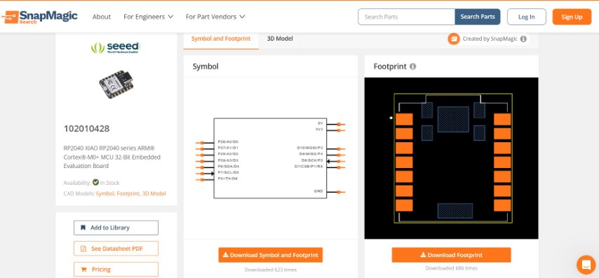
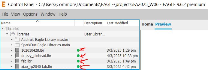
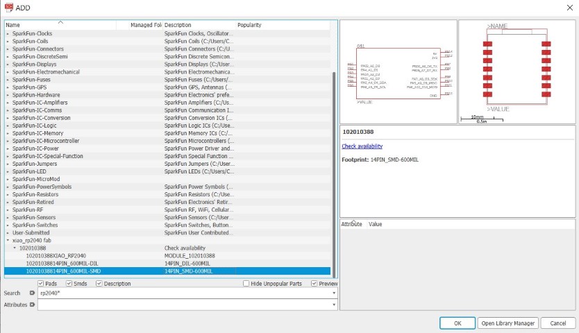
After installing Autodesk EAGLE, the very first thing that I do is to download all the important Libraries, such as fab.lbr (most common components can be found in this library) and 102010428.lbr (SEEED XIAO RP2040 symbol and footprint).


Do not forget to select USE option for both libraries after right click and the drop down list occurs. That particular library will have a GREEN light beside the library list.
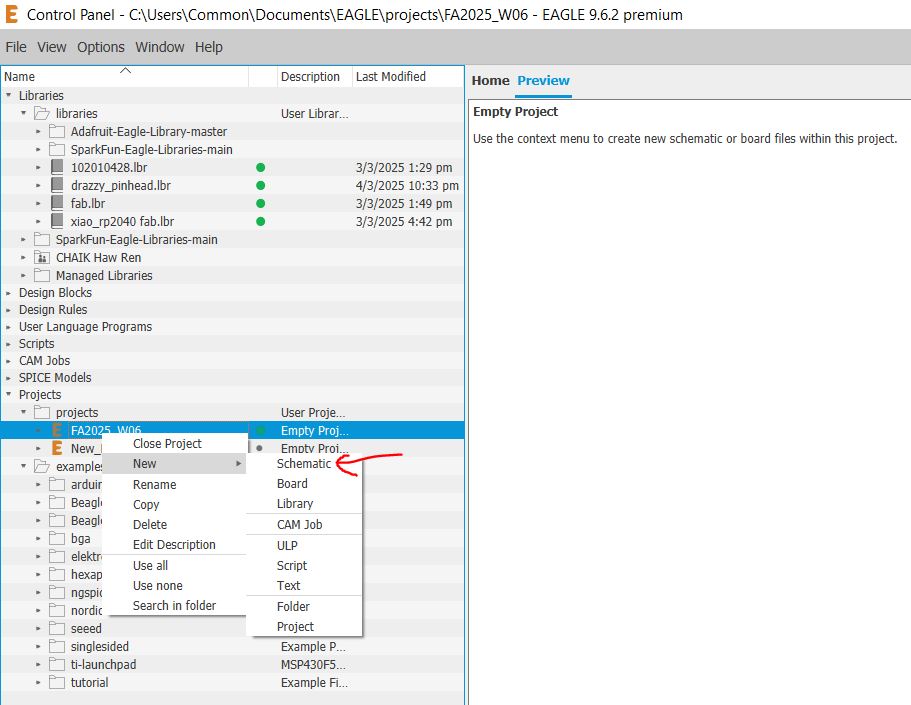
Here are the process to create a schematic diagram: PROJECT > NEW PROJECT > Name your Project Folder > Right click on your Project Folder > Select SCHEMATIC, a new, blank window should immediately pop up.

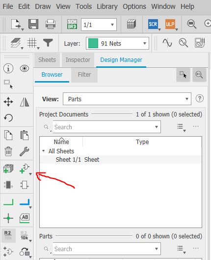
Adding Parts to a Schematic Diagram

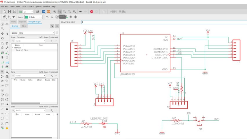
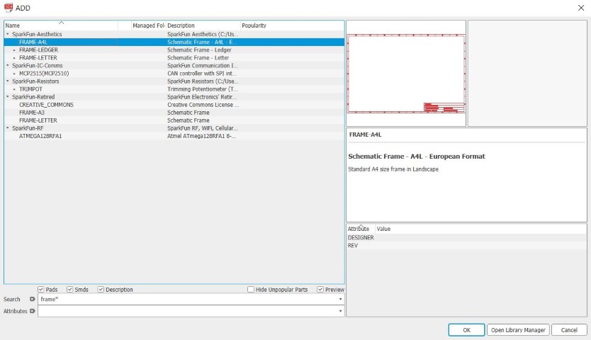
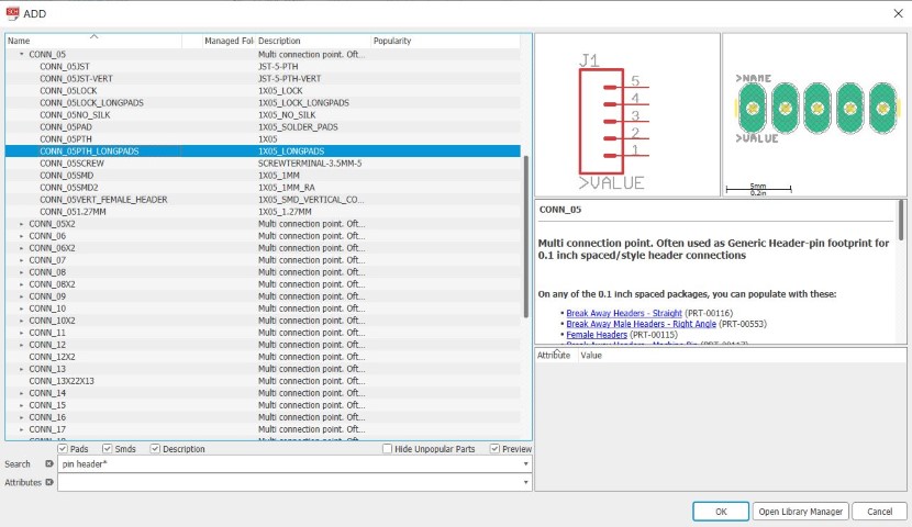
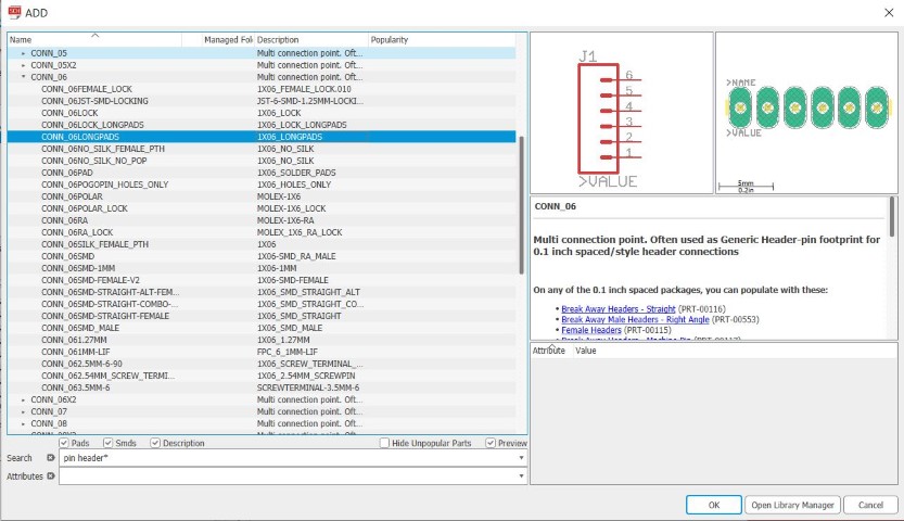
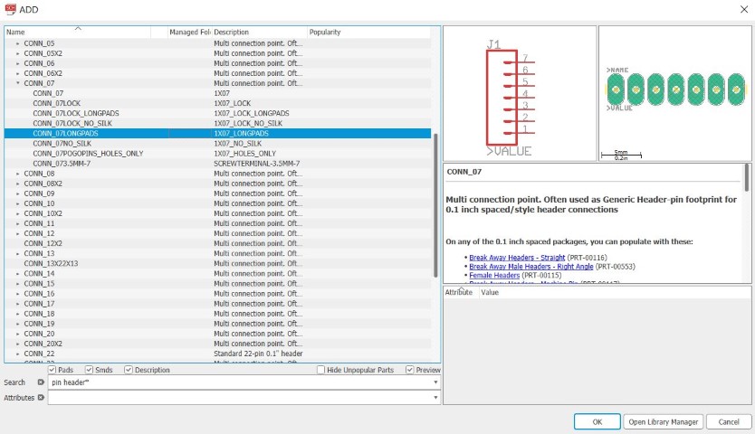
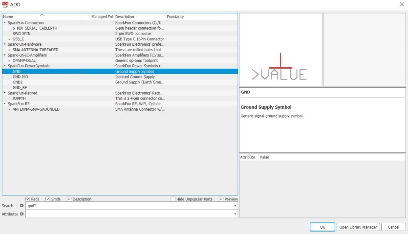
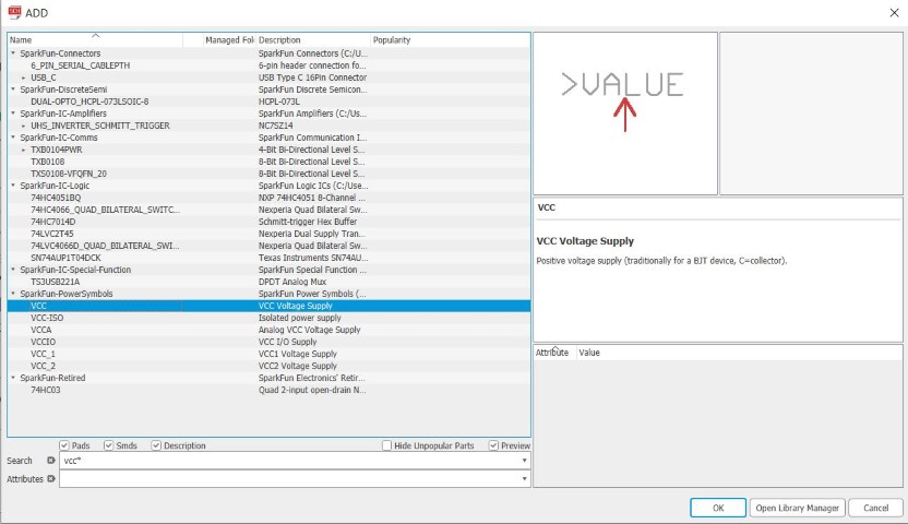
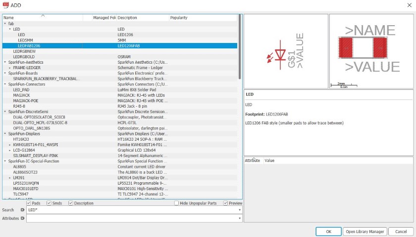
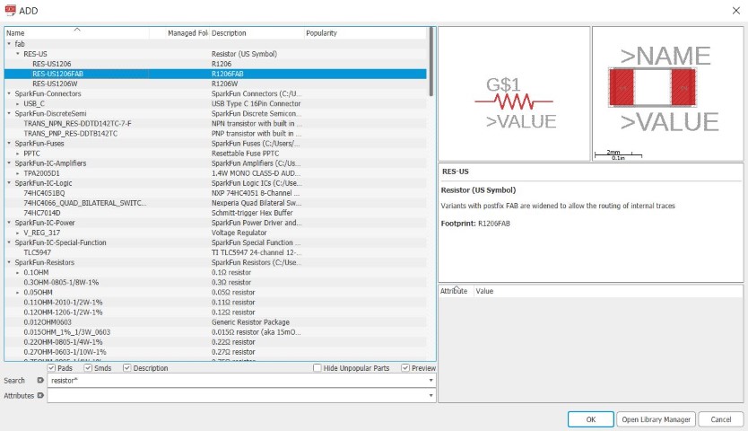
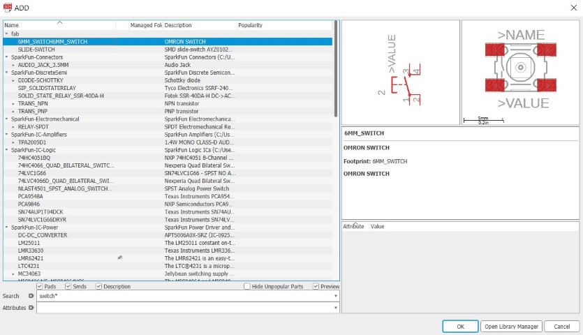
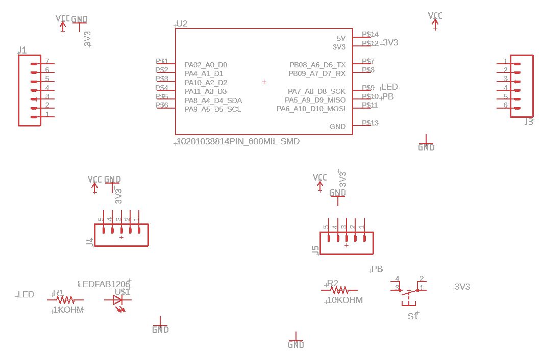
Adding a FRAME --> Adding a Micro-controller (SEEED XIAO RP2040 - 102010428.lbr) --> Adding a few Pin Headers --> Adding Power Inputs (VCCs and GNDs) --> Adding Supporting Circuitries (LED, Resistors and Push Button).


Wiring up the Schematic diagram

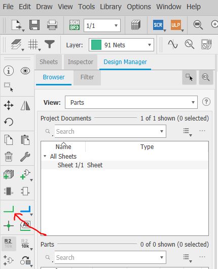
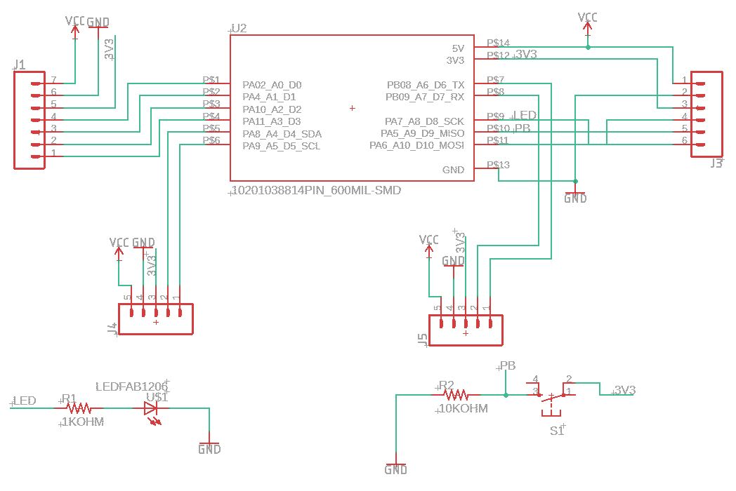
Using NET tool instead of WIRE tool to route all the components in the schematic diagram (Line in GREEN). Route the POWER INPUT CIRCUITS --> Route the MICRO-CONTROLLER --> Route the rest of the components that should be linked to the development board --> Making Name and Label Net Stubs. (Text in GREY)

Creating a board from schematic
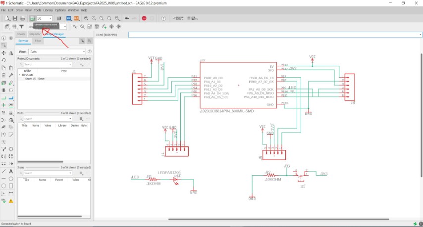
To switch from the schematic editor to the related board, simply click the Generate/Switch to Board command

which should prompt a new, board editor window to open. All of the parts you added from the schematic should be there, stacked on top of each other, ready to be placed and routed.

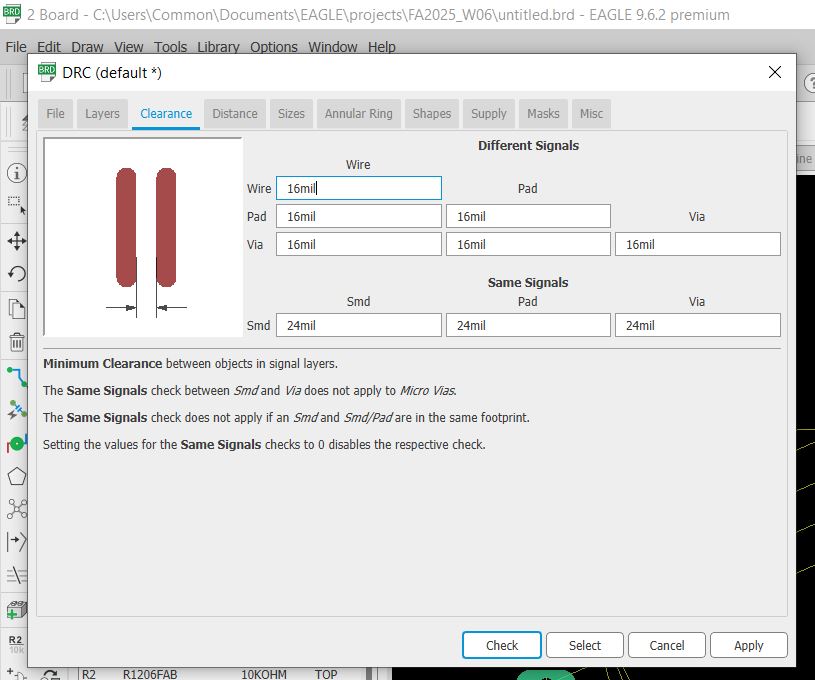
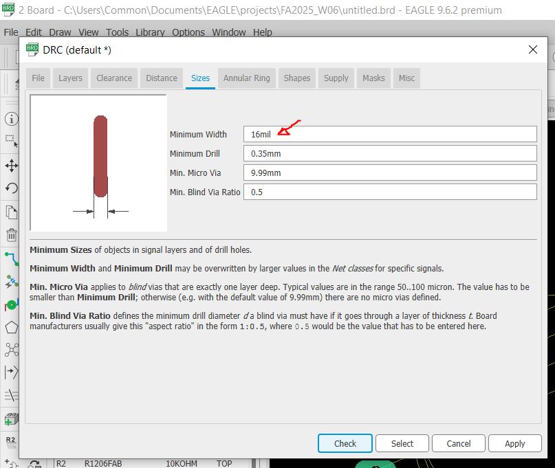
Before start routing the pins, we need to preset the settings in DRC (Design Rules Check).


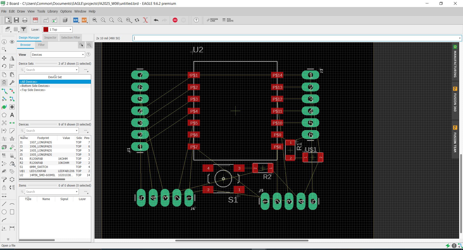
Let's start routing the board.
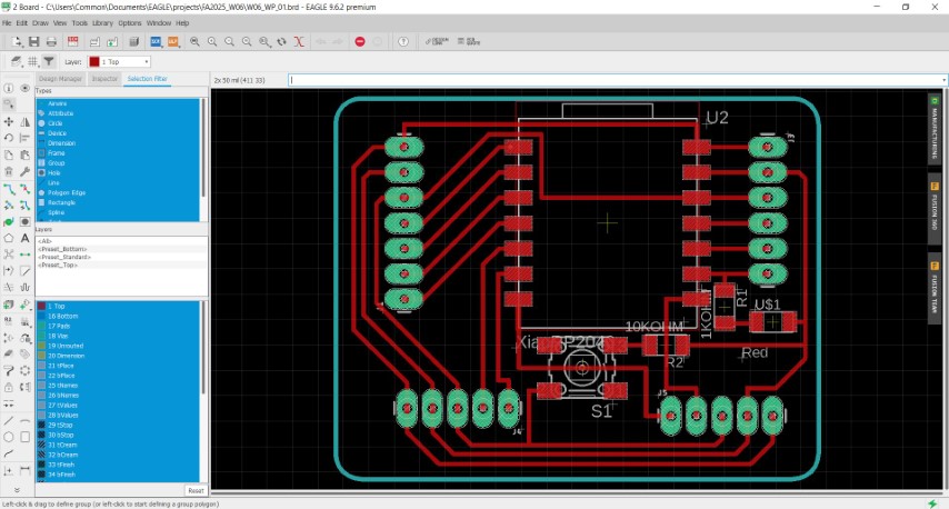
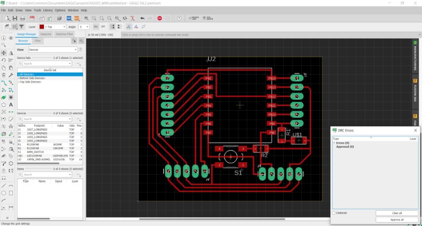
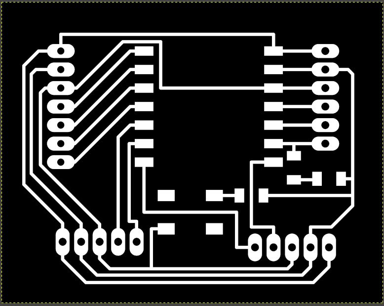
I am using both STRAIGHT LINES and MOVING THE COMPONENTS to route them together. As a start up, I am using AUTOROUTER to plan my board routing. From there, I will try to re-design the route that are in BLUE to make them turn RED. As a beginner, it tooks me almost 2 days to complete this session. Here is my final board layout:

Checking for Errors
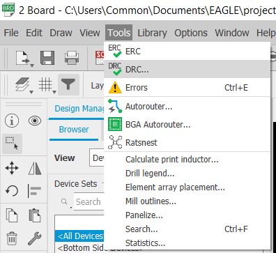
Return back to TOOLS > DRC option to check my board if got any errors. If occurs any errors, I need to troubleshoot them before export to PNG file and generate G-CODE by using MODS software.

Export PNG Image to Generate G-CODE
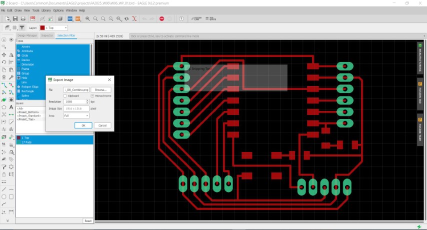
While exporting my final PCB PNG image, I need to:
1. Name the PNG file for CNC machining.
2. Select Monochrome.
3. Set the Resolution value. Typically the figure range from 1000 to 2000dpi. For my case, I will choose 1000 dpi.

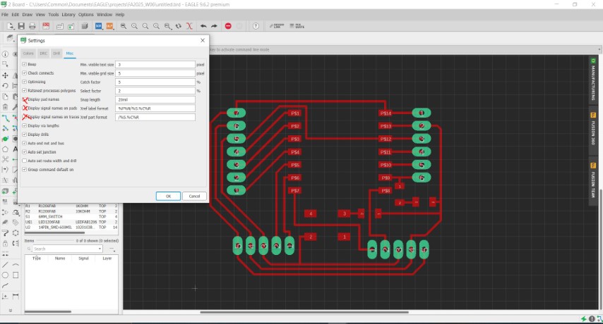
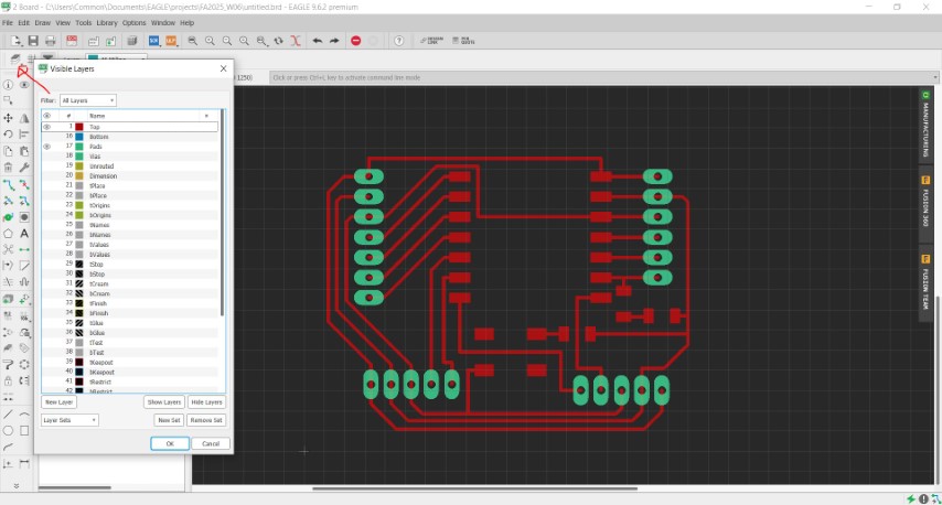
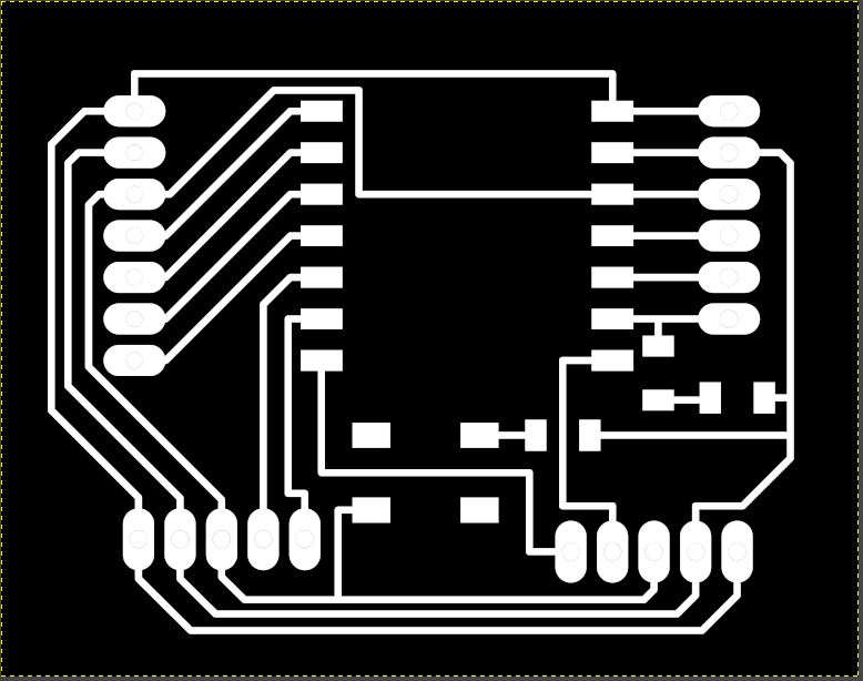
Before exporting the image, ensure that only the TRACED path and PAD are shown in the final diagram. Go to OPTIONS > Set... > Setting screen and uncheck "Display pad names", "Display signal names on pads" and "Display signal names on trace". Also, select ONLY "#1 Top layer" and "#17 Pads layer". You may export the PNG file into separate files - One file is for tracing, and the other file is for pads.


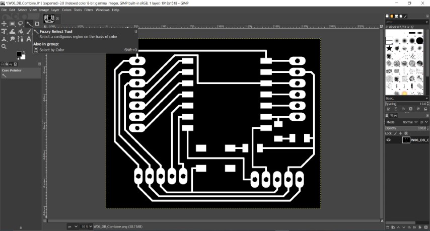
There are adidtional work to be done before CNC machining my PNG image file for PADS. All the holes need to be covered up before sending for machining. To fill up the pad holes: Open GIMP apps > Open the file > Select "FUZZY SELECT TOOL" at the left hand options > Press "SHIFT" button and select the holes that need to be covered >


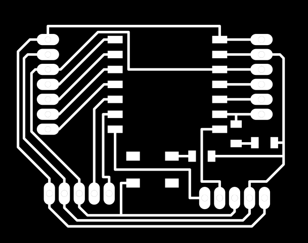
Same for the milling process to vector cut out the PCB.


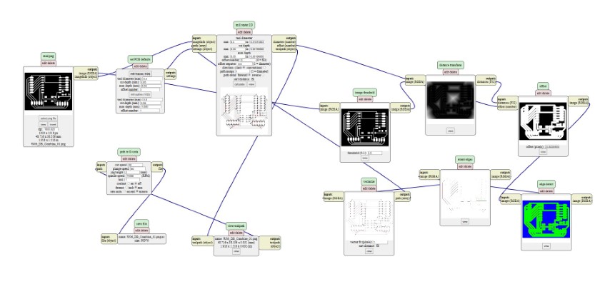
Once I have the PNGs, I follow the steps below to generate the G-code file from the mods page:
1. Open the MODS PAGE.
2. Right click on the screen and choose PROGRAMS from the menu.
3. Then choose SERVER PROGRAM from the list.
4. Scroll down to G-code, chose mill 2D PCB png.
5. Once Mods windows are open, select OPEN PNG file for trace file.
6. At the third window we select CALCULATE.
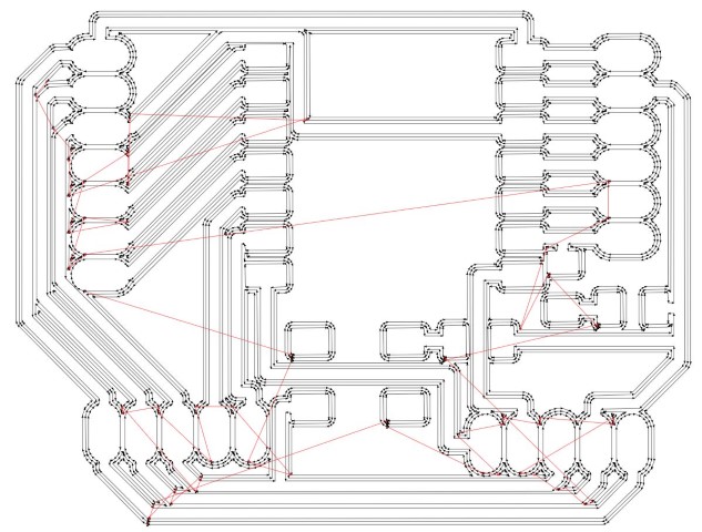
7. Select VIEW to see the G-code path.


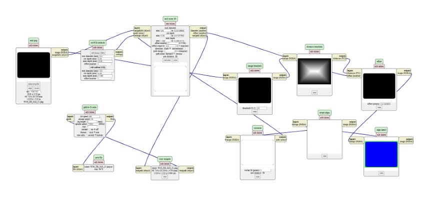
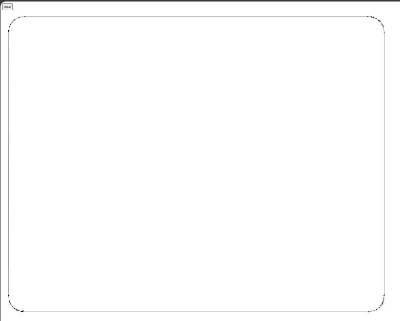
Same applies to milling process for outline cut.


Reflection
Being new to this topic, I am struggling to cope with the knowledge and skill sets that supposed to be picking up for this week. Both my repo and the documentation are not up to the minimal standard that can be accepted as a whole. I would mostly spend a little bit of this week time to turn back to fine tune the repo, at least make it understandable for myself to make my own printed circuit board for my final project.
